Product Specifications
Manufacturer: AMD Xilinx
Part Number: XC7Z010-1CLG400C
Product Type: System on Chip (SoC) / FPGA
Family: Zynq-7000
Core Processor: Dual ARM Cortex-A9 MPCore with CoreSight
Processor Speed: 667 MHz
Logic Cells (PL): 28,000
DSP Slices (PL): 80
Block RAM (PL): 240 KB
On-Chip RAM (PS): 256 KB
Programmable I/O (PL): 100
Processor I/O (PS MIO): 54
Speed Grade: -1
Process Technology: 28 nm
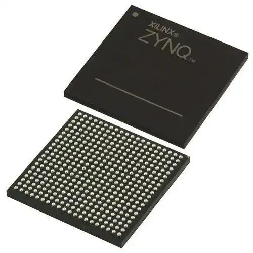
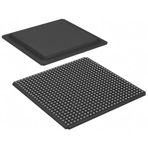
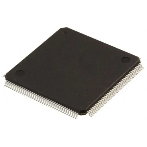
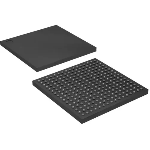
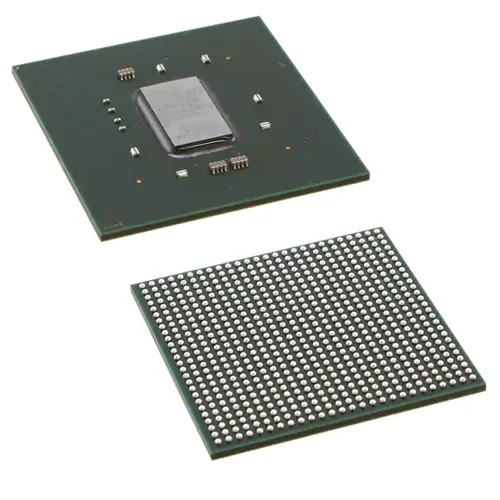
Package: 400-CSPBGA (17x17 mm)
Operating Temperature: 0°C to 85°C
Product Description
The XC7Z010-1CLG400C is not just an FPGA. It is not just a microcontroller. It is both, in the same physical package, connected by an internal high‑bandwidth bus that makes the two halves look like a single chip to software.
Processing System vs. Programmable Logic
The PS (Processing System) side contains a dual‑core ARM Cortex-A9 MPCore processor running at 667 MHz, with 256 KB of on‑chip RAM, cache controllers, interrupt handling, and standard peripherals — USB, Ethernet, UART, SPI, I²C, GPIO, and memory controllers for DDR3. You write C/C++ code for this side, just like any other ARM processor. Linux runs here. FreeRTOS runs here. Bare‑metal applications run here.
The PL (Programmable Logic) side is essentially an Artix-7 FPGA with 28,000 logic cells, 80 DSP slices, 240 KB of block RAM, and 100 dedicated I/O pins. You program this side in Verilog or VHDL, just like any other FPGA. The magic is that the PL can connect directly to the PS through a high‑bandwidth AXI bus interface — up to hundreds of megabytes per second — without going off‑chip.
Why This Architecture Exists
Traditional embedded systems use a microcontroller and a separate FPGA on the same PCB. Data crosses from one chip to the other through a narrow SPI or parallel bus — slow, power‑hungry, and physically large. The Zynq-7000 puts the two chips onto one piece of silicon, with an internal bus that is both faster and lower power. The 17×17 mm CSPBGA package is smaller than many standalone ARM processors alone, let alone a two‑chip solution.
The XC7Z010 is the entry point to the Zynq-7000 family. It has fewer logic cells than the XC7Z020 (28,000 vs 85,000) and fewer DSP slices (80 vs 220). But for many applications — motor control with hardware acceleration, industrial Ethernet gateways, vision processing with simple algorithms — 28,000 logic cells are enough. The real value is not the size of the PL, but the fact that it exists at all alongside a 667 MHz dual‑core ARM.
What People Build with This
Consider a drone flight controller: the ARM runs the navigation stack (sensor fusion, waypoint tracking, communication with ground control), while the PL handles the real‑time motor control loops and sensor capture. No latency from an external bus. Or a software‑defined radio: the ARM runs the protocol stack, the PL does the digital downconversion and filtering. Or an industrial gateway: ARM runs Linux and network stacks, PL implements custom fieldbus protocols.
If your design can get by with a smaller ARM processor or a smaller FPGA separately, that might be cheaper. But if you need both a capable processor and customizable hardware logic in a compact footprint — and you want them to talk to each other at internal bus speeds — the Zynq-7000 is difficult to beat.
Resources & Documentation
The Chip That Puts an ARM CPU and an FPGA on the Same Die – Xilinx Zynq-7000 XC7Z010-1CLG400C
Product Specifications
Manufacturer: AMD Xilinx
Part Number: XC7Z010-1CLG400C
Product Type: System on Chip (SoC) / FPGA
Family: Zynq-7000
Core Processor: Dual ARM Cortex-A9 MPCore with CoreSight
Processor Speed: 667 MHz
Logic Cells (PL): 28,000
DSP Slices (PL): 80
Block RAM (PL): 240 KB
On-Chip RAM (PS): 256 KB
Programmable I/O (PL): 100
Processor I/O (PS MIO): 54
Speed Grade: -1
Process Technology: 28 nm
Package: 400-CSPBGA (17x17 mm)
Operating Temperature: 0°C to 85°C
Resources & Documentation
Xilinx XC7K160T-1FBG676C
Kintex-7 FPGA 162K cells
Xilinx XC2C32A-6VQG44C
CoolRunner-II CPLD 32MC 5.5ns
Xilinx XC9572XL-10TQG100C
XC9500XL CPLD 72MC 10ns
Xilinx XC3S50AN-4TQG144I
Industrial Spartan-3AN FPGA 50K
Xilinx XC3S200AN-4FTG256I
Industrial Spartan-3AN FPGA 200K

Xilinx XC95144XL-10TQG100I
Industrial temp XC9500XL CPLD 144MC

Xilinx XC6SLX9-2FTG256C
Spartan-6 LX 9K cells FTBGA
Xilinx XC5VLX30-1FFG676C
Virtex-5 LX FPGA 30K cells