
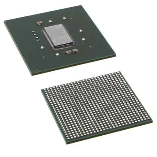
Product Specifications
- Manufacturer
- Xilinx (AMD)
- Part Number
- XC5VLX30-1FFG676C
- Product Type
- Field Programmable Gate Array (FPGA)
- Series
- Virtex-5 LX
- Logic Cells
- 30,720
- Logic Blocks (CLBs)
- 2,400
- System Gates
- 30,000
- Number of I/O
- 400
- Total RAM Bits
- 1,179,648
- Speed Grade
- -1
- Maximum Frequency
- 550 MHz
- Process Technology
- 65 nm CMOS
- Supply Voltage
- 0.95 V – 1.05 V
- Package
- 676-FCBGA (27x27 mm)
- Operating Temperature
- 0°C to 85°C (TJ)
Product Description
The Xilinx XC5VLX30-1FFG676C is a mid-range member of the Virtex-5 LX FPGA family, offering 30,720 logic cells and 1.18 Mb of block RAM in a 676-pin FCBGA package. Built on 65 nm CMOS technology and operating at a core voltage of 1.0 V, this device delivers up to 550 MHz performance, providing a high-performance programmable logic platform for advanced system designs.
Architecture
The Virtex-5 LX family uses the second-generation ASMBL (Advanced Silicon Modular Block) column-based architecture, containing five distinct platforms. Each platform contains a different ratio of features to address the needs of a wide variety of advanced logic designs. The XC5VLX30-1FFG676C features 30,720 logic cells organised into 2,400 configurable logic blocks (CLBs), providing flexible logic implementation for complex system designs.
Memory and DSP Resources
The device incorporates powerful 36-Kbit block RAM/FIFOs totalling 1,179,648 bits of on-chip memory, enabling high-bandwidth data storage for demanding applications. The second-generation 25 x 18 DSP slices provide efficient digital signal processing acceleration for arithmetic functions and filtering algorithms. The device also integrates system monitor functionality for on-chip voltage and temperature monitoring.
I/O and Clock Management
The device provides 400 user I/O pins supporting a wide range of single-ended and differential signalling standards through SelectIO technology with built-in digitally-controlled impedance. ChipSync source-synchronous interface blocks simplify high-speed data capture. Enhanced clock management tiles with integrated DCM (Digital Clock Managers) and PLL (Phase-Locked Loop) clock generators provide precise frequency synthesis and phase control. The device features up to eight low-skew global clock networks.
Technical Specifications
| Parameter | Value |
| Logic Cells | 30,720 |
| Logic Blocks (CLBs) | 2,400 |
| Number of I/O | 400 |
| Total RAM Bits | 1,179,648 |
| Maximum Frequency | 550 MHz |
| Process Technology | 65 nm CMOS |
| Supply Voltage | 0.95V – 1.05V |
Packaging and Environmental
The XC5VLX30-1FFG676C is housed in a 676-pin FCBGA (Flip-Chip Ball Grid Array) package measuring 27 x 27 mm. The package is RoHS compliant and lead free. Moisture Sensitivity Level is MSL 3, requiring a floor life of 168 hours after opening. The device is supplied in tray packaging with 21 pieces per tray.
Development Support
The Virtex-5 family is supported by Xilinx ISE Design Suite (ISE 14.7). The device is not supported by the newer Vivado toolchain, which targets 7-series and later devices. Programming is performed via JTAG (IEEE 1149.1) using standard cables. The device supports advanced configuration options including partial reconfiguration and bitstream encryption.
Product Status
The XC5VLX30-1FFG676C is currently active and available from distributors. For new designs requiring similar performance with modern tool support, consider the Kintex-7 or Artix-7 families, which offer improved power efficiency and Vivado compatibility.
Resources & Documentation
The High‑Performance Mid‑Range Virtex‑5 – Xilinx XC5VLX30-1FFG676C
Product Specifications
- Manufacturer
- Xilinx (AMD)
- Part Number
- XC5VLX30-1FFG676C
- Product Type
- Field Programmable Gate Array (FPGA)
- Series
- Virtex-5 LX
- Logic Cells
- 30,720
- Logic Blocks (CLBs)
- 2,400
- System Gates
- 30,000
- Number of I/O
- 400
- Total RAM Bits
- 1,179,648
- Speed Grade
- -1
- Maximum Frequency
- 550 MHz
- Process Technology
- 65 nm CMOS
- Supply Voltage
- 0.95 V – 1.05 V
- Package
- 676-FCBGA (27x27 mm)
- Operating Temperature
- 0°C to 85°C (TJ)
Resources & Documentation
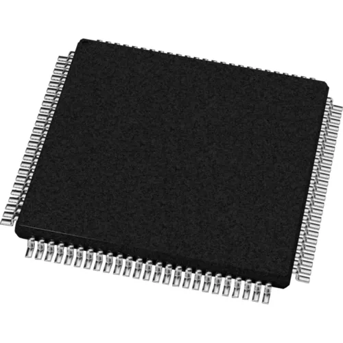
Xilinx XC95144XL-7TQG100C
XC9500XL CPLD 144MC 7.5ns
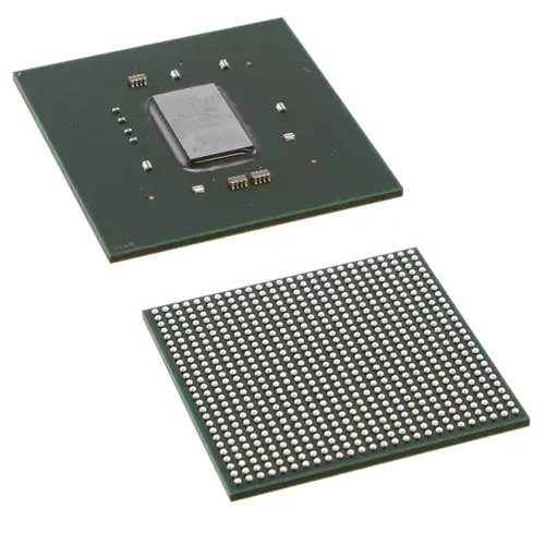
Xilinx XC7A100T-2FGG484I
Industrial Artix-7 FPGA 101K cells
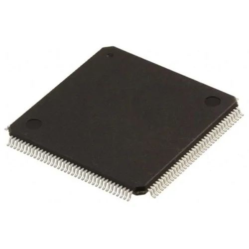
Xilinx XC3S400-4TQG144C
Spartan-3 FPGA 400K gates

Xilinx XCKU040-2FFVA1156E
Kintex UltraScale FPGA 530K cells
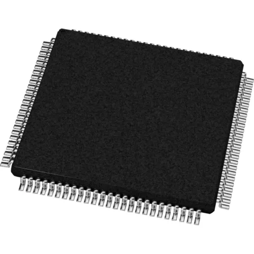
Xilinx XC95144XL-10TQG100C
XC9500XL CPLD 144MC 100MHz
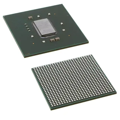
Xilinx XC6SLX75-3FGG484C
Spartan-6 LX 74K cells 862MHz
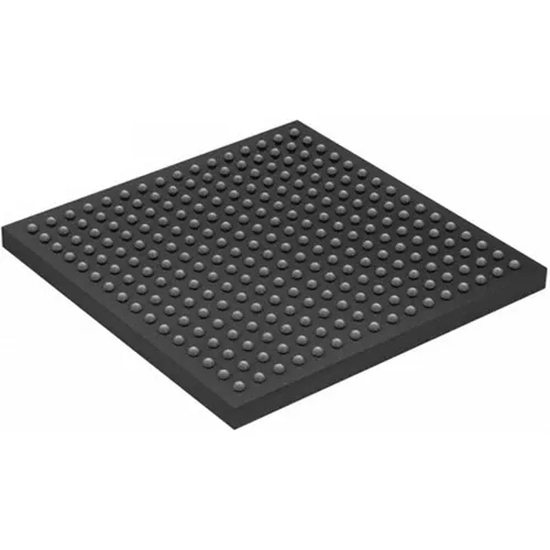
Xilinx XC6SLX16-2FTG256C
Spartan-6 LX FPGA 14K cells
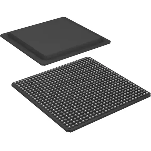
Xilinx XC6SLX100-3FGG676C
Spartan-6 LX FPGA 100K cells
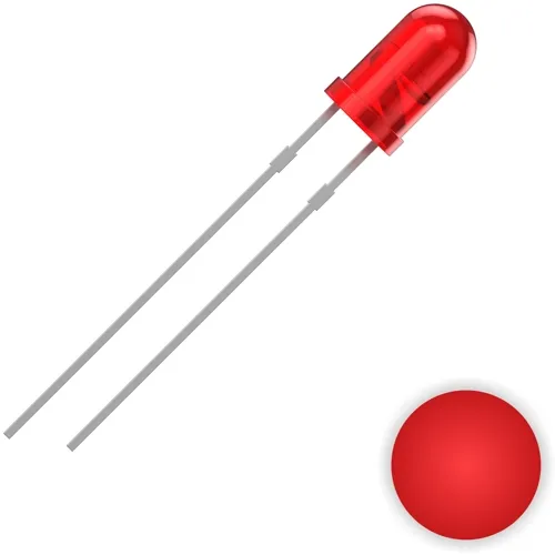
QUADRIOS 2111O155
Classic red for alerts
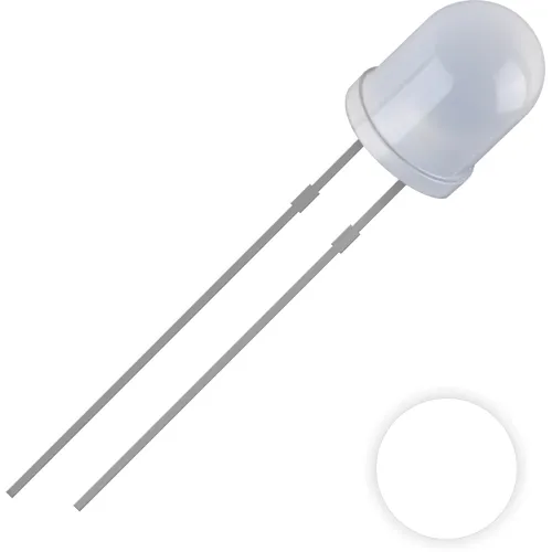
QUADRIOS 2111O167
Bright white for illumination
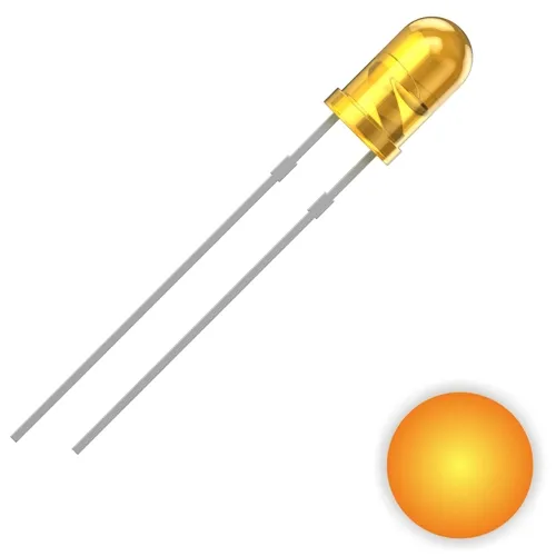
QUADRIOS 2111O154
Basic yellow for status lights
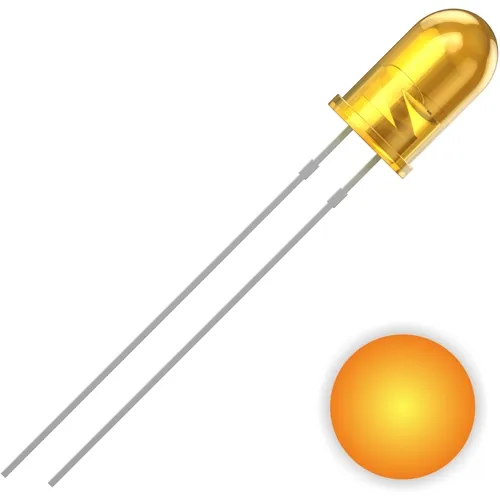
QUADRIOS 2111O159
Classic yellow for status panels
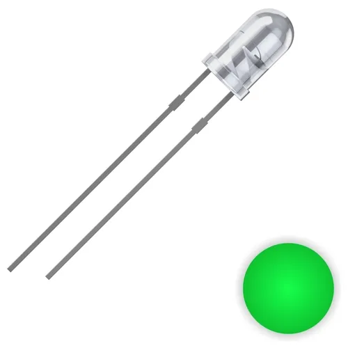
QUADRIOS 2111O176
Extreme brightness for signs
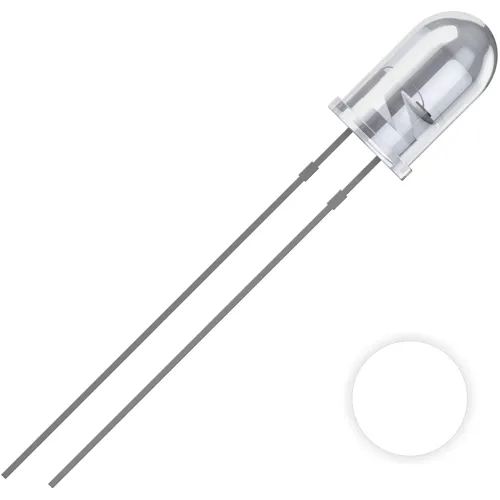
QUADRIOS 2111O182
Extreme brightness for signage
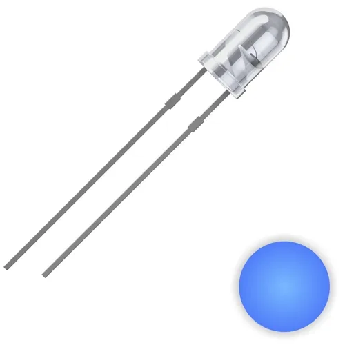
QUADRIOS 2111O175
Focused blue for long distance
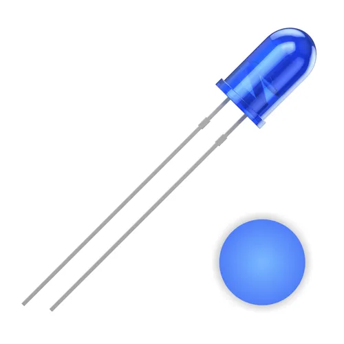
QUADRIOS 2111O156
Deep blue for clear contrast