Product Specifications
Manufacturer: Xilinx (AMD)
Part Number: XC7K160T-1FBG676C
Product Type: Field Programmable Gate Array (FPGA)
Series: Kintex-7
Logic Cells: 162,240
Logic Blocks (LABs/CLBs): 12,675
Number of I/O: 400
Total RAM Bits: 11,980,800
Speed Grade: -1
Maximum Clock Frequency: 1098 MHz
Process Technology: 28 nm CMOS
Supply Voltage: 0.97 V – 1.03 V
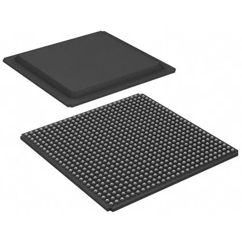
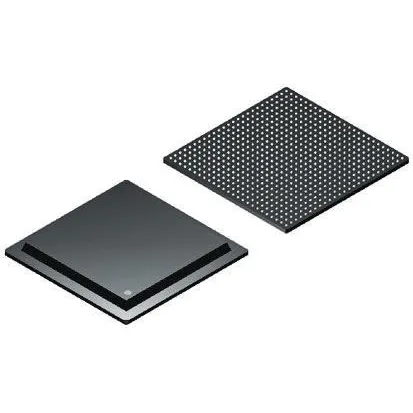
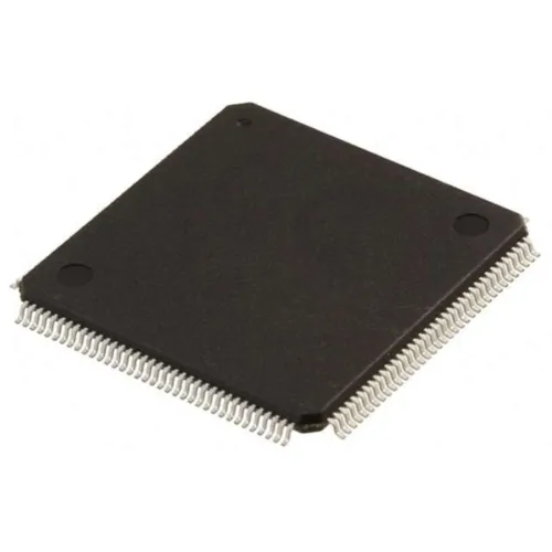
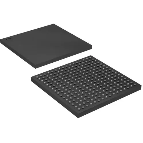
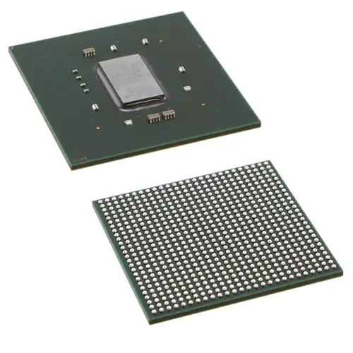
Package: 676-FBGA (27x27 mm)
Operating Temperature: 0°C to 85°C
Product Description
The Xilinx XC7K160T-1FBG676C is a member of the Kintex-7 FPGA family, delivering the optimal balance of performance, power consumption, and cost for high-volume applications. Built on 28 nm CMOS technology and operating at a core voltage of 1.0 V, this device features 162,240 logic cells and a maximum clock frequency of 1098 MHz, making it suitable for communications infrastructure, data center acceleration, and advanced signal processing applications.
Architecture
The XC7K160T-1FBG676C features 162,240 logic cells organised into 12,675 configurable logic blocks (CLBs), providing substantial logic capacity for complex system designs. The Kintex-7 family offers a rich selection of built-in system-level blocks including DSP48E1 slices for digital signal processing acceleration, block RAM for on-chip data storage, and high-speed serial transceivers for advanced connectivity.
Memory and DSP Resources
The device incorporates 11,980,800 bits of block RAM, enabling large on-chip data storage for high-bandwidth applications. Integrated DSP48E1 slices support 25 x 18 multiply-accumulate operations, providing efficient implementation of arithmetic functions and filtering algorithms. The memory controller blocks support a wide range of memory interfaces including DDR3 and QDRII.
High-Speed Connectivity
The device provides 400 user I/O pins, supporting a wide range of single-ended and differential signalling standards. High-speed serial transceivers support data rates up to 12.5 Gb/s, making the device suitable for PCI Express, Gigabit Ethernet, and other high-bandwidth interfaces. The Kintex-7 family includes PCI Express compliant Endpoint blocks for integrated serial connectivity.
Technical Specifications
| Parameter | Value |
| Logic Cells | 162,240 |
| Logic Blocks (LABs/CLBs) | 12,675 |
| Number of I/O | 400 |
| Total RAM Bits | 11,980,800 |
| Maximum Clock Frequency | 1098 MHz |
| Process Technology | 28 nm CMOS |
| Supply Voltage | 0.97V – 1.03V |
Packaging and Environmental
The XC7K160T-1FBG676C is housed in a 676-pin FBGA (Fine-Pitch Ball Grid Array) package measuring 27 x 27 mm. Moisture Sensitivity Level is MSL 3, requiring a floor life of 168 hours after opening. The device is supplied in tray packaging.
Development Support
The Kintex-7 family is supported by AMD Vivado Design Suite, which provides a comprehensive development environment for design entry, synthesis, implementation, and debug. The device supports partial reconfiguration and advanced design security features. For high-speed serial connectivity designs, Vivado IP Integrator provides pre-verified IP blocks for PCI Express, Ethernet, and other protocols.
Product Status
The XC7K160T-1FBG676C is currently active and available from distributors. The device remains in active production and is suitable for new designs requiring high-performance programmable logic. For volume production, verify lead times and availability with authorised distributors.
Resources & Documentation
162K Logic Cells of Kintex-7 Power – Xilinx XC7K160T-1FBG676C
Product Specifications
Manufacturer: Xilinx (AMD)
Part Number: XC7K160T-1FBG676C
Product Type: Field Programmable Gate Array (FPGA)
Series: Kintex-7
Logic Cells: 162,240
Logic Blocks (LABs/CLBs): 12,675
Number of I/O: 400
Total RAM Bits: 11,980,800
Speed Grade: -1
Maximum Clock Frequency: 1098 MHz
Process Technology: 28 nm CMOS
Supply Voltage: 0.97 V – 1.03 V
Package: 676-FBGA (27x27 mm)
Operating Temperature: 0°C to 85°C
Resources & Documentation
Xilinx XC2C32A-6VQG44C
CoolRunner-II CPLD 32MC 5.5ns
Xilinx XC9572XL-10TQG100C
XC9500XL CPLD 72MC 10ns
Xilinx XC3S50AN-4TQG144I
Industrial Spartan-3AN FPGA 50K
Xilinx XC3S200AN-4FTG256I
Industrial Spartan-3AN FPGA 200K

Xilinx XC95144XL-10TQG100I
Industrial temp XC9500XL CPLD 144MC

Xilinx XC6SLX9-2FTG256C
Spartan-6 LX 9K cells FTBGA
Xilinx XC5VLX30-1FFG676C
Virtex-5 LX FPGA 30K cells

Xilinx XC2C128-7VQG100C
CoolRunner-II CPLD 128MC 7ns
CAEN Spa V2495
Altera Cyclone V, 32 gate/delay, VME64X